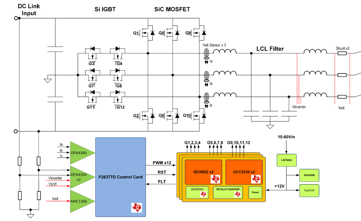
10kW ЫЋЯђШ§ЯрШ§МЖsic CAR CHARGERВЮПМЩшМЦ
етвЛОЙ§бщжЄЕФВЮПМЩшМЦИХЪіСЫШчКЮЪЕЁЛЯжЛљгк SiC ЕФШ§МЖШ§ЯржБСї/НЛСї T аЭІчФцБфЦїМЖЁЃ50KHz ЕФНЯИпПЊЙиЦЕТЪМѕаЁСЫТЫВЈЦїЩшМЦЕФДХаддЊМўГпДчЃЌВЂвђДЫЬсИпСЫЙІТЪУмЖШЁЃЭЈЙ§ЪЙгУПЩНЕЕЭПЊЙиЫ№КФЕФ SiC MOSFETЃЌПЩШЗБЃЪЕЯжИпДя 1000V ЕФИќИпжБСїзмЯпЕчбЙКЭИќЕЭЕФПЊЙиЫ№КФЃЌДгЖјДяЕН 99% ЕФЗхжЕаЇТЪЁЃДЫЩшМЦПЩХфжУЮЊСНМЖЛђШ§МЖФцБфЦїЁЃИУЯЕЭГгЩЕЅИі C2000 ЮЂПижЦЦї (MCU) TMS320F28379D НјааПижЦЃЌПЩдкЫљгадЫааФЃЪНЯТЮЊЫљгаЕчдДЕчзгПЊЙиЦїМўЩњГЩ PWM ВЈаЮЁЃ
Ьиад
- ЖюЖЈБъГЦЪфШыЕчбЙ/зюДѓЪфШыЕчбЙЃК800V/1000VDC
- дк 400VAC 50/60Hz T аЭСЌНгЪБЕФзюЁНДѓЪфГіЙІТЪЮЊ 10kW/10KVA
- ЙЄзїЪБЕФЙІТЪвђЪ§ЗЖЮЇЮЊ 0.7 жЭКѓжС 0.7 ГЌЧА
- ЛљгкИпбЙ (1200V) SiCMosFET ЕФШЋЁаЁЁЧХФцБфЦїЃЌЗхжЕаЇТЪИпДя 99%
- ТњдиЪБЕФЪфГіЕчСї THD аЁгк 2%
- ЪЙгУ AMC1301 НјааИєРыЪНЕчЁсСїМьВтЃЌДгЖјЪЕЯжИКдиЕчСїМрВт
гУгкЧ§ЖЏИпбЙ SiC MOSFET ВЂОпгадіЧПаЭИєРыЙІФмЕФИєРыЪНЧ§ЁПЖЏЦї ISO5852SЃЌвдМАгУгкЧ§ЖЏжаЁКМфЈ Si IGBT ЕФ UCC5320S
2 System Overview 2.1 Block Diagram Figure 2-1. TIDA-01606 Block Diagram This reference design is comprised of four separate boards that intercommunicate. The following boards work in tandem to form this three-phase inverter reference design: ? A power board, comprising all of the switching device, LCL filter, sensing electronics, and power structure ? A TMS320F28379D Control Card to support the DSP ? Three gate driver cards, each with two ISO5852S and two UCC5320 gate drivers ? A DC bus voltage measuring board (TIDA-01606 ISOHVCARD)

2.2 Highlighted Products 2.2.1 ISO5852S The ISO5852S device is a 5.7-kVRMS, reinforced isolated gate driver for IGBTs and MOSFETs with split outputs, OUTH and OUTL, providing 2.5-A source and 5-A sink current. The input side operates from a single 2.25-V to 5.5-V supply. The output side allows for a supply range from minimum 15 V to maximum 30 V. Two complementary CMOS inputs control the output state of the gate driver. The short propagation time of 76 ns provides accurate control of the output stage. ? 100-kV/ІЬs minimum common-mode transient immunity (CMTI) at VCM = 1500 V ? Split outputs to provide 2.5-A peak source and 5-A peak sink currents ? Short propagation delay: 76 ns (typ), 110 ns (max) ? 2-A active Miller clamp ? Output short-circuit clamp ? Soft turnoff (STO) during short circuit ? Fault alarm upon desaturation detection is signaled on FLT and reset through RST ? Input and output undervoltage lockout (UVLO) with Ready (RDY) pin indication ? Active output pulldown and default low outputs with low supply or floating inputs ? 2.25-V to 5.5-V input supply voltage ? 15-V to 30-V output driver supply voltage www.ti.com System Overview TIDUE53G ЈC MARCH 2018 ЈC REVISED SEPTEMBER 2022 Submit Document Feedback 10-kW, Bidirectional Three-Phase Three-Level (T-type) Inverter and PFC Reference Design 3 Copyright ? 2022 Texas Instruments Incorporated? CMOS compatible inputs ? Rejects input pulses and noise transients shorter than 20 ns ? Operating temperature: ЈC40ЁуC to +125ЁуC ambient ? Isolation surge withstand voltage of 12800-VPK GND1 VEE2 RST RDY FLT IN+ INЁР VCC1 VCC2 DESAT GND2 OUTH OUTL CLAMP VCC1 VCC1 UVLO1 Mute Decoder Q SR Q VCC1 VCC1 Gate Drive and Encoder Logic UVLO2 2 V 9 V 500 ІЬA STO VCC2 Ready Fault Figure 2-2. ISO5852S Functional Block Diagram 2.2.2 UCC5320 The UCC53x0 is a family of compact, single-channel, isolated IGBT, SiC, and MOSFET gate drivers with superior isolation ratings and variants for pinout configuration, and drive strength. The UCC53x0 is available in an 8-pin SOIC (D) package. This package has a creepage and clearance of 4 mm and can support isolation voltage up to 3 kVRMS, which is good for applications where basic isolation is needed. With these various options and wide power range, the UCC53x0 family is a good fit for motor drives and industrial power supplies. ? 3-V to 15-V input supply voltage ? 13.2-V to 33-V output driver supply voltage ? Feature options: ЈC Split outputs (UCC5320S and UCC5390S) ЈC UVLO with respect to IGBT emitter (UCC5320E and UCC5390E) ЈC Miller clamp option (UCC5310M and UCC5350M) ? Negative 5-V handling capability on input pins ? 60-ns (typical) propagation delay for UCC5320S, UCC5320E, and UCC5310M ? 100-kV/ІЬs minimum CMTI ? Isolation surge withstand voltage: 4242 VPK ? Safety-related certifications: ЈC 4242-VPK isolation per DIN V VDE V 0884-10 and DIN EN 61010-1 (planned) ЈC 3000-VRMS isolation for 1 minute per UL 1577 (planned) ЈC CSA Component Acceptance Notice 5A, IEC 60950-1 and IEC 61010-1 End Equipment Standards (Planned) ЈC CQC Certification per GB4943.1-2011 (Planned) System Overview www.ti.com 4 10-kW, Bidirectional Three-Phase Three-Level (T-type) Inverter and PFC Reference Design TIDUE53G ЈC MARCH 2018 ЈC REVISED SEPTEMBER 2022 Submit Document Feedback Copyright ? 2022 Texas Instruments Incorporated? 4-kV ESD on all pins ? CMOS inputs ? 8-pin narrow body SOIC package ? Operating temperature: ЈC40ЁуC to +125ЁуC ambient text VCC2 UVLO, Level Shift and Control Logic VCC2 VOUTH INЁР IN+ VOUTL VCC1 VEE2 GND1 UVLO and Input Logic 15 V Rest of Circuit 5 V Figure 2-3. UCC5320 Functional Block Diagram (S Version) 2.2.3 TMS320F28379D The Delfino? TMS320F2837xD is a powerful 32-bit floating-point microcontroller unit (MCU) designed for advanced closed-loop control applications such as industrial drives and servo motor control; solar inverters and converters; digital power; transportation; and power line communications. Complete development packages for digital power and industrial drives are available as part of the powerSUITE and DesignDRIVE initiatives. While the Delfino product line is not new to the TMS320C2000? portfolio, the F2837xD supports a new dual-core C28x architecture that significantly boosts system performance. The integrated analog and control peripherals also let designers consolidate control architectures and eliminate multiprocessor use in high-end systems. ? Dual-core architecture: ЈC Two TMS320C28x 32-bit CPUs ЈC 200 MHz ЈC IEEE 754 single-precision floating-point unit (FPU) ЈC Trigonometric math unit (TMU) ЈC Viterbi/complex math unit (VCU-II) ? Two programmable control law accelerators (CLAs) ЈC 200 MHz ЈC IEEE 754 single-precision floating-point instructions ЈC Executes code independently of main CPU ? On-chip memory ЈC 512KB (256 kW) or 1MB (512 kW) of Flash (ECC-protected) ЈC 172KB (86 kW) or 204KB (102 kW) of RAM (ECC-protected or parity-protected) ЈC Dual-zone security supporting third-party development ? Clock and system control: ЈC Two internal zero-pin 10-MHz oscillators ЈC On-chip crystal oscillator ЈC Windowed watchdog timer module ЈC Missing clock detection circuitry ? 1.2-V core, 3.3-V I/O design ? System peripherals: ЈC Two external memory interfaces (EMIFs) with ASRAM and SDRAM support ЈC Dual six-channel direct memory access (DMA) controllers

