0755-28286748
Xilinx? 7 series FPGAs comprise four FPGA families that address the complete range of system requirements, ranging from low cost, small form factor, cost-sensitive, high-volume applications to ultra high-end connectivity bandwidth, logic capacity, and signal processing capability for the most demanding high-performance applications. The 7 series FPGAs include:
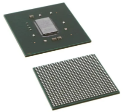
Zynq-7000 SoC First Generation Architecture The Zynq?-7000 family is based on the Xilinx SoC architecture. These products integrate a feature-rich dual-core or single-core ARM? Cortex?-A9 based processing system (PS) and 28 nm Xilinx programmable logic (PL) in a single device. The ARM Cortex-A9 CPUs are the heart of the PS and also include on-chip memory, external memory interfaces, and a rich set of peripheral connectivity interfaces. Processing System (PS) ARM Cortex-A9 Based Application Processor Unit (APU) ? 2.5 DMIPS/MHz per CPU ? CPU frequency: Up to 1 GHz ? Coherent multiprocessor support ? ARMv7-A architecture ? TrustZone? security ? Thumb?-2 instruction set ? Jazelle? RCT execution Environment Architecture ? NEON? media-processing engine ? Single and double precision Vector Floating Point Unit (VFPU) ? CoreSight? and Program Trace Macrocell (PTM) ? Timer and Interrupts ? Three watchdog timers ? One global timer ? Two triple-timer counters Caches ? 32 KB Level 1 4-way set-associative instruction and data caches (independent for each CPU) ? 512 KB 8-way set-associative Level 2 cache (shared between the CPUs) ? Byte-parity support On-Chip Memory ? On-chip boot ROM ? 256 KB on-chip RAM (OCM) ? Byte-parity support External Memory Interfaces ? Multiprotocol dynamic memory controller ? 16-bit or 32-bit interfaces to DDR3, DDR3L, DDR2, or LPDDR2 memories ? ECC support in 16-bit mode ? 1GB of address space using single rank of 8-, 16-, or 32-bit-wide memories ? Static memory interfaces ? 8-bit SRAM data bus with up to 64 MB support ? Parallel NOR flash support ? ONFI1.0 NAND flash support (1-bit ECC) ? 1-bit SPI, 2-bit SPI, 4-bit SPI (quad-SPI), or two quad-SPI (8-bit) serial NOR flash 8-Channel DMA Controller ? Memory-to-memory, memory-to-peripheral, peripheral-to-memory, and scatter-gather transaction support I/O Peripherals and Interfaces ? Two 10/100/1000 tri-speed Ethernet MAC peripherals with IEEE Std 802.3 and IEEE Std 1588 revision 2.0 support ? Scatter-gather DMA capability ? Recognition of 1588 rev. 2 PTP frames ? GMII, RGMII, and SGMII interfaces ? Two USB 2.0 OTG peripherals, each supporting up to 12 Endpoints ? USB 2.0 compliant device IP core ? Supports on-the-go, high-speed, full-speed, and low-speed modes ? Intel EHCI compliant USB host ? 8-bit ULPI external PHY interface ? Two full CAN 2.0B compliant CAN bus interfaces ? CAN 2.0-A and CAN 2.0-B and ISO 118981-1 standard compliant ? External PHY interface ? Two SD/SDIO 2.0/MMC3.31 compliant controllers ? Two full-duplex SPI ports with three peripheral chip selects ? Two high-speed UARTs (up to 1 Mb/s) ? Two master and slave I2C interfaces ? GPIO with four 32-bit banks, of which up to 54 bits can be used with the PS I/O (one bank of 32b and one bank of 22b) and up to 64 bits (up to two banks of 32b) connected to the Programmable Logic ? Up to 54 flexible multiplexed I/O (MIO) for peripheral pin assignments Interconnect ? High-bandwidth connectivity within PS and between PS and PL ? ARM AMBA? AXI based ? QoS support on critical masters for latency and bandwidth control
���� ҽ�� 5G ��Ƶ����
| �ͺ� | DataSheet | Dimension (mm) | Description |
|---|

 ��оƬ��MCU
 ģ�⨎�ͽӿ�оƬ
 MEMS������
 ��ͨWIFIоƬ